Boards for this project were sponsored by PCBWay (affiliate link).
Playing with electronics means dealing with a lot of protocols. Be it UART, RS-232, I2C, or CAN-bus, I have made a version to fit my Framework laptop. However, one popular protocol was strangely absent - RS-485. Well, it’s time to correct that mistake.
Since I successfully used JST XH with many Framework expansion cards before, connector decision was easy. However, deciding which pinout to use was a bit more troublesome as I needed 3 pins and common wisdom was that order is GND-A-B. However, my UART cards were using 3-pin setup with GND in middle. It would be too easy to forget which card was plugged in and get the most crucial pin wrong.
So, the only remaining choice was to have A-GND-B order but I really didn’t like it and honestly I am not sure why. It’s a good pinout allowing for excellent routability (since protection diodes have this pinout already). But no other RS-485 device has it. While moving GND pin to center would alleviate error rate among my framework expansion cards, I could see even myself accidentally connecting ground to the first pin.
At the end I decided to use 4-pin socket with the last pin pulled out. This would allow for standard GND-A-B setup while making connector distinctively different from my cards that use center pin for GND. Even better, GND signal here actually matches my CAN-bus card where that last pin is populated (albeit not used).
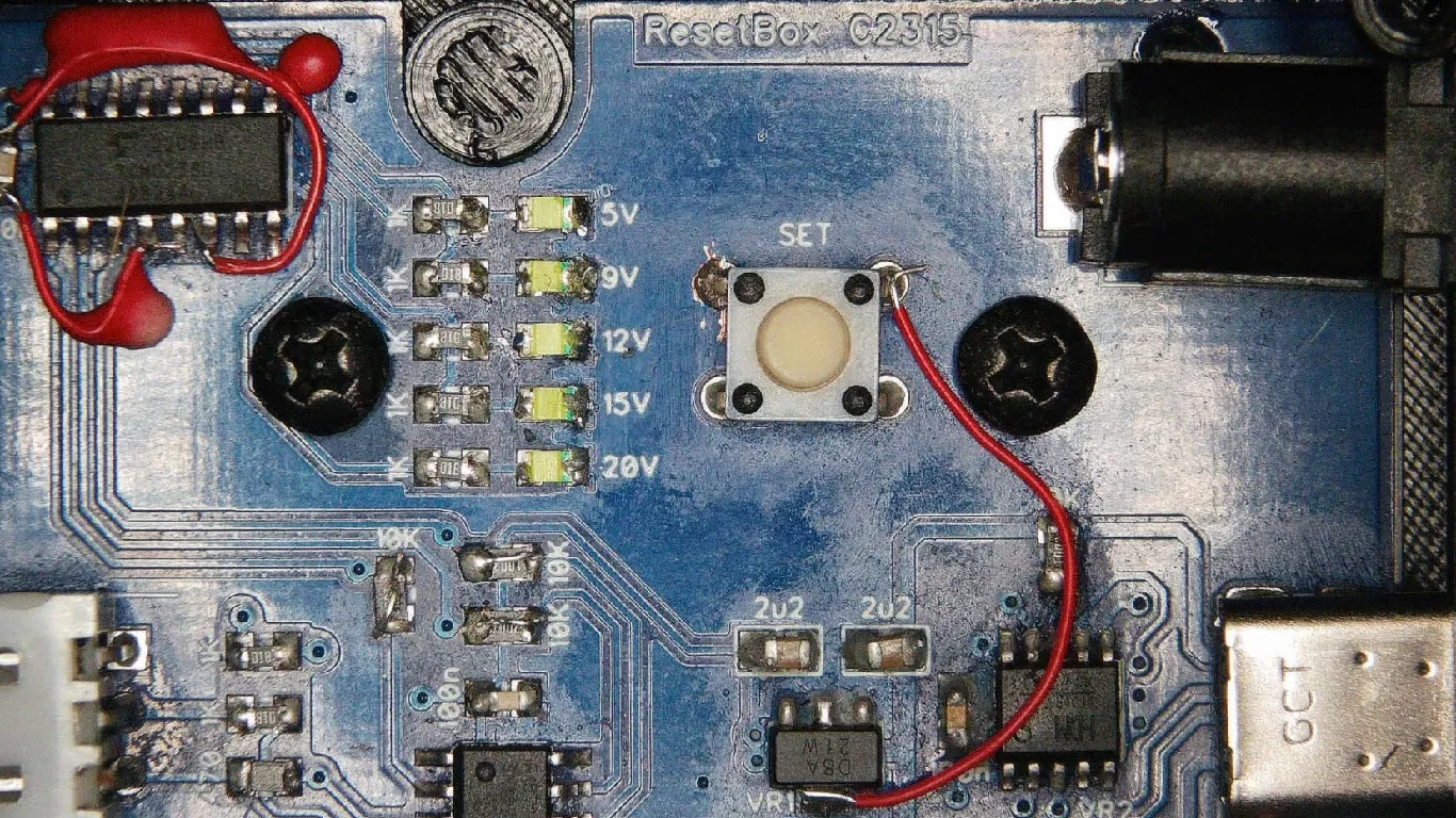
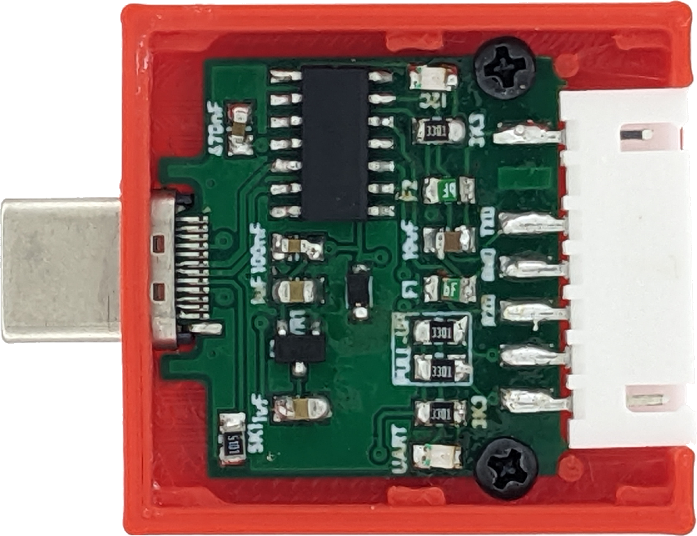
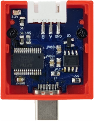
Since I still had bunch of SP485EN chips I used for another project, it was easy to select RS-485 transceiver. And honestly, while aged, it’s not a bad chip for the purpose. It’s available from multiple sources, it has low pin count in easily hand-solderable package, and at 5 Mbps it’s way faster than UART I was planning to pair it with.
Speaking of UARTs, there is one that you will find mentioned time and time again when it comes to RS-485 - FTDI FT232RL. And that’s for a good reason. It’s a single chip solution without the need for crystal, allows for reasonably high baud rates, and it has specialized TXDEN pin allowing for automatic flow control. While its pin count might be on a high side and comes with a bit of baggage, it really fits nicely for the purpose.
While FT232 does offer reasonably full RS-485 schematics, I added a few things to spice it all up. First of all, I added a MOSFET to keep RS-485 transceiver fully off when in USB suspend. I later did find this was not really necessary as SP485EN has a suspend mode that FT232 can nicely trigger, it does offer me a bit of flexibility for further testing.
Another thing I added were biasing resistors. In my own setups I found that this increases bus resiliency a lot and it only costs you 3 resistors. What value resistors? Well, that’s where it gets tricky. There are so many ways to calculate these resistor values and you need to know a lot about the exact setup in order to make it perfect. Since I wanted to use this device in many different networks, the best I could hope for is to get close enough. In this case this meant 130/750Ω combination. When combined with 120Ω termination on the other side of the bus, it should handle many scenarios.
For protection, I decided to use good old SM712 TVS diodes to keep SP485EN safe and a few fast fuses on both data lines and on the ground for catastrophe prevention. Ideally you might want to have an isolated interface between your laptop and any bus. However, I simply didn’t have enough space on board for discrete solution and solutions with integrated DC-DC converter were either way to expensive or unobtainable.
While fuses are not ideal replacement for isolation since bad things can still happen if you deal with wildly different potentials, things are not as bleak as it’s easy to insulate your laptop. Simply unplugging it from its power supply and running it of battery will do the trick and allow you safe interfacing.
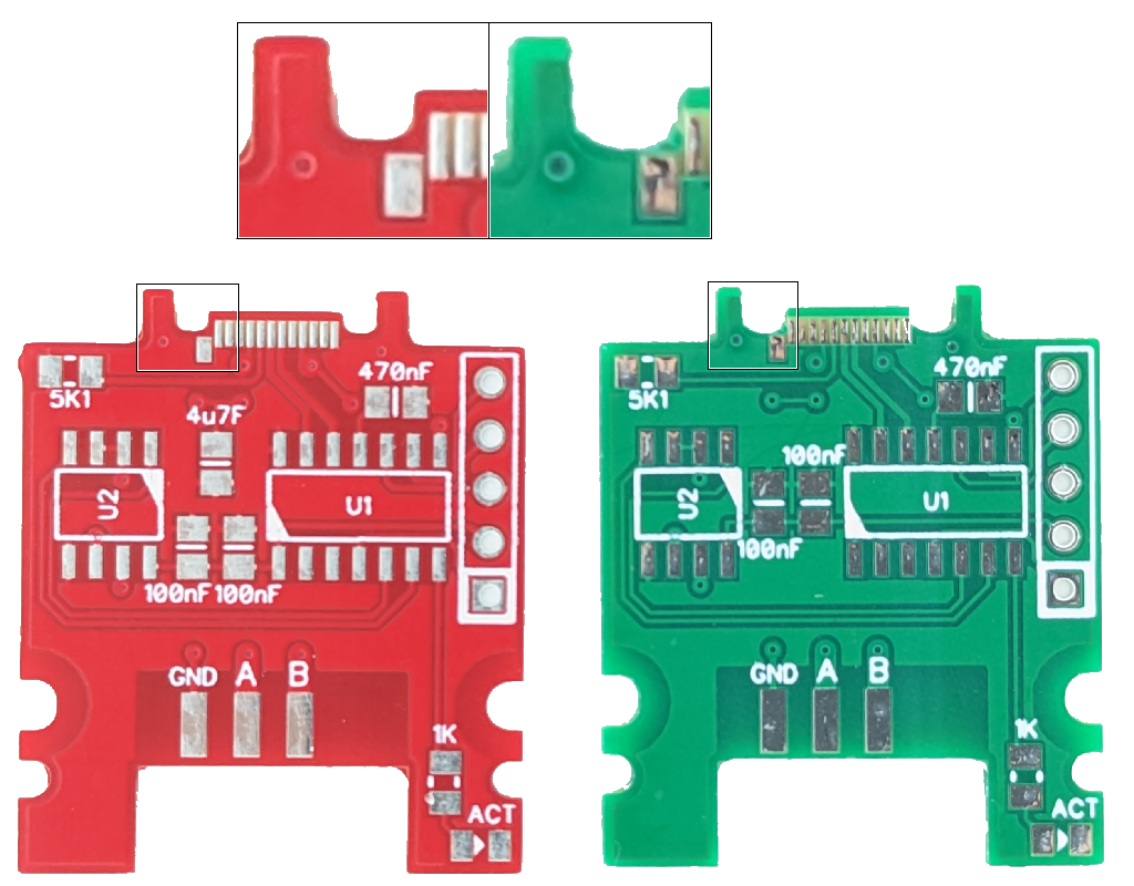
With the overall design done, I turned to PCB fabrication and PCBWay. I decided to go with them due to previous good experiences when it came to Framework expansion boards. While they are simple enough, routing them properly is a bit tricky. Only once I already made an order did PCBWay come back and proposed a sponsorship in the form of free PCBs. And that jinxed it, I guess, since for the first time routing was not ok.
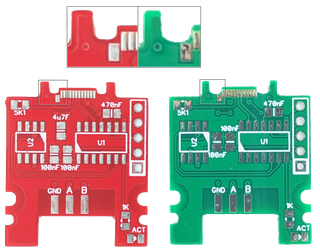
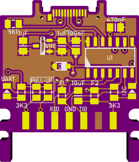
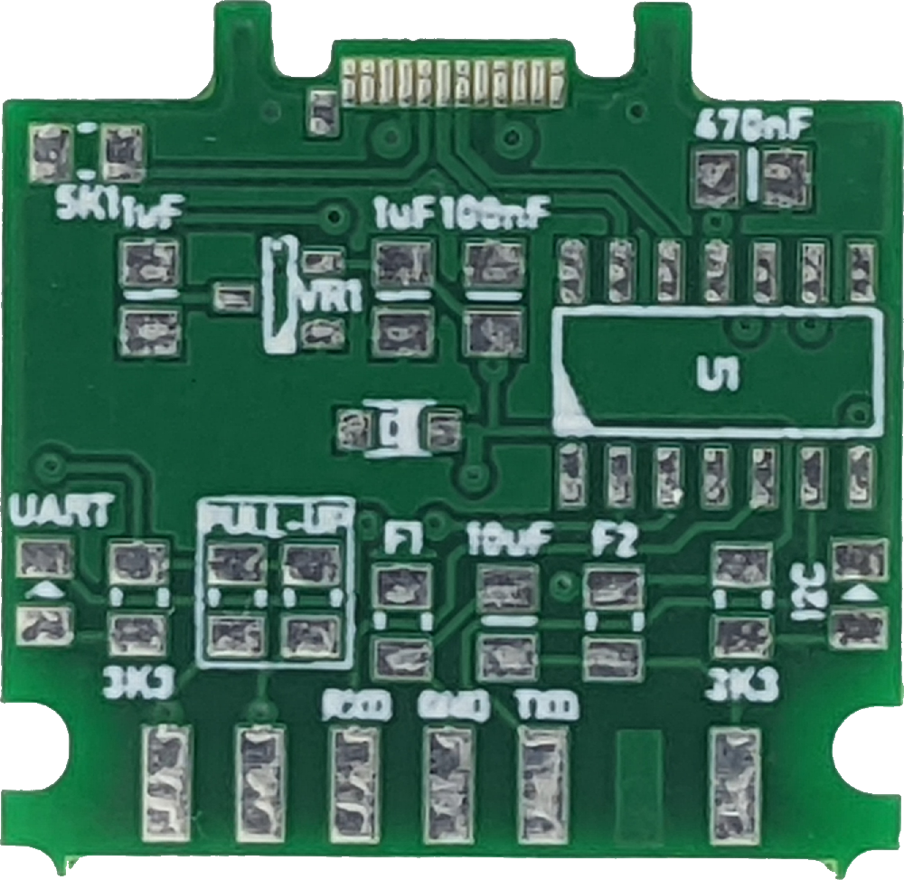
Per my understanding, most commonly fabs do board edge routing with a 1.6 mm or larger mill end. This is done for both speed and durability as smaller bits do tend to break more. Routing boards intended for type-C connector used here requires 1.0 mm or smaller bit in order to properly do the notches. If you check the bad board (green) and compare it to the good board (red), you’ll see how little difference there is.
In any case, that gave me an opportunity to deal with their helpdesk for the first time. After writing a ticket, I got a response in less than 24 hours despite them being in holiday time. After a short back-and-forth where I got to explain the exact problem, I had my updated order with extra notes attached. And yes, I selected a different color so I don’t mix them up.
When it comes to the PCB quality, there isn’t much I can say I haven’t said before. A default HASL finish is good enough and there were no leveling issues. If you want ENIG, that is an option albeit quoted price skyrockets when selected. Soldermask is decent and can handle lead-free soldering temperatures without issues. I usually go fora green color as it has the shortest lead time, but you can select other 5 colors at no extra cost (purple and matte colors are extra).
Silk screen is of decent quality and resolution even for small font sizes. And yes, PCBWay still adds their identification number on board by default with option to remove it requiring $1.50. For these boards I don’t really care since they won’t be visible to the end user but if you want to do user-facing panels, you might want to pay extra.
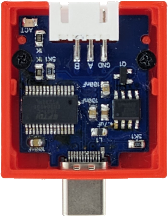
With all components soldered, I connected it to a Framework laptop and the experience was as good as you can get. One great advantage of FTDI chips is that they work flawlessly. I tested it on a few small RS-485 busses at varying speeds (up to 1 Mbaud) without any communication issues. Even under scope things were looking good.
But, is there a way to get rid of FTDI? Well, we can discuss that in the next instalment of the RS-485 Framework expansion card saga. :)
As always, you can find project on GitHub