Bad things happen when programmer finds a soldering iron

RS-232 Framework Expansion Card

A while ago I created a CAN-bus expansion card for Framework laptop. However, I consider this an utter failure. While the card did work, the lack of CAN-bus capable parts meant you cannot actually create one yourself. At least until this IC shortage comes to an end. However, experience was fun enough that I decided to make something else I do need and that one could actually manufacture in today’s world - a RS-232 expansion card.

For those uninitiated, RS-232 is an overall standard that defined connection between different devices for a long time. As many standards go, RS-232 is quite an expansive beast with many different signals. However, over the time, it became really common to have it boiled down to a three-wire setup: RXD (receive), TXD (transmit), and GND (ground). While RS-232 did disappear from desktops and laptops alike, it’s far from dead. Be it industrial equipment or a network switch, RS-232 still has its place.

Illustration

Design was easy enough. To get from USB to TTL UART, I used MCP2221, but any similar chip will work equally well. Resulting TTL signal is then fed into MAX232 where charge pump brings it to RS-232 voltage levels, about ±8 V. This is quite sufficient to be fully RS-232 compliant. Even better, MAX232 will allow for receiving a full RS-232 ±15V signal with some margin. The end result should be that you can interconnect with pretty much any RS-232 compliant device out there.

Unlike for my CAN-bus expansion card, here I went for a slightly bigger connector of JST XH variety. While this one actually required a bit of modification to the expansion card casing, it’s actually much more convenient than its 2.0 mm brethren. First of all, spacing is 2.5 mm which is close enough to 0.1" spacing that you can easily use a standard jumper wires to connect. This means you don’t need any specialized tools or bother with creating a cable yourself. Further more, if you plan to have something more permanent connected and you want the polarity protection you get from JST XH, it’s trivial to find many cables with 3-pin JST XH already present.

Illustration

Pinout was another difficult choice and in the end I decided onto RXD GND TXD. Benefits of this approach are mostly in the area of safety. If GND wire was at pin 1, there is some place for doubt whether you start counting on left or right. With it being in the middle, that doubt is removed. Further more, to do the self-test, one just needs to connect two outer pins together. Again, it describes connection uniquely without even mentioning pin numbers. Yes, you need pin numbers for RXD and TXD regardless but swapping those two will never cause any damage so the guessing game is less dangerous.

Illustration

As noted above, the boards were manufactured by PCBWay and there were a few things to watch out for. Due to the connector, these boards had to be 0.8mm. PCBWay does support this thickness without any extra cost and it’s only a click away.

Another thing to watch for, was that this board really does require 6/6 manufacturing process. Interestingly, I accidentally had one via that was too close but my board passed all the checks PCBWay had. When I got it back, I saw that via’s ring was adjusted to be slightly thinner on the offending side so everything ended up working just fine. While I appreciate such help, I would actually prefer the check to fail so I can correct the boards myself instead of silently fixing the issue.

One important thing that had me worried was if small PCB features needed for USB type-C edge connector would be routed correctly. What I discovered by accident was that some board houses do their routing with a 0.068" mill end which is a bit too large for these cutouts. If that happens, you simply cannot fit this connector onto it. What you want is 0.04" mill end to correctly handle this board outline. Either someone was paying attention or PCBWay does this by default. Either way, I got my boards perfectly milled.

If you look at pictures carefully, you will also notice something is off with the silk screen and here I must take a full fault for this. I do love Bahnschrift font and how well it renders at small sizes so I decided to use it for silk-screen markings. But I got greedy and went with its condensed variant that, in retrospective, had no chance of being readable. This one was purely on me.

In any case, boards were in my hands within 10 days. This also meant they arrived faster than I was ready for them but I cannot really hold this against PCBWay. :)

Illustration

As far as case goes, I toyed with an idea to fit it into the existing USB A case. While this might have been just possible, it also meant for each device one would need to dismantle a perfectly good official expansion card. Thus, I went with 3D printed case with slight modifications. When combined with friction-fit top, card actually doesn’t look half bad.

With everything else out of the way, now comes the part where I tell you about potential issues. The major one is that this is non-insulated interface. RS-322 driver can easily handle ±30 V so this would not be an issue normally. However, for signals to be measured, one needs to have both communicating devices on the same ground potential. And therein lies the major trouble. If you accidentally connect something that is not ground into this, you will pass a significant current and maybe burn down the transceiver. In the worst case you could also damage the laptop as all grounds are connected together.

All that said, as long as you connect ground to ground you should be fine. If you are not sure about the ground potential on the other side, a neat trick is to simply disconnect your laptop from the AC adapter. If you run your laptop of the battery, its ground will “float” and thus you again can rely on ±30 V range of MAX232 chip. This simple trick will give you enough leeway to make many mistakes.

Lastly, there is a slightly unconventional fast (20 ms) fuse on the ground path that might save your butt if things go really bad. Notice that I said “might” and not “will” here. Fuses are great but even a fast fuse will take a decent amount of time to break the connection. Fortunately, type-C ports are quite rugged so odds are decent the motherboard won’t be damaged. But I wouldn’t bet on it.

Illustration

My personal approach when connecting anything to this expansion card would be to make sure I’m connecting ground on both sides and, as an extra precaution, to test connection with laptop disconnected for the mains. If communication works fine, you can connect laptop back to the mains.

Also note this is nothing specific to this adapter - all non-insulated USB adapters (and most of them are) suffer from the same potential problems. However, due to the size of this expansion card, it’s much easier to misconnect wires then when you’re connecting to the DB-9.

In any case, as always, the design is freely available. If you don’t want to bother soldering one yourself, they are also available for purchase (USA only, at this time).

CyberCard

Illustration

As I got another CyberPower UPS for my devices, I again decided to use a custom card to connect it to my computer. However, using my existing PCB was a no-go as chip shortage meant my bellowed Si8621 was unobtanium again. Well, I guess it was time to have it redesigned anyhow…

For those joining the party late, this custom card is intended for the CyberPower expansion slot thus allowing for a more direct query and control interface than what you usually get from the 1U UPS range. Benefit of this approach is that you can script whatever support you want for you operating system without having to deal with CyberPower’s software (or, in case of Linux, lack there of).

Fortunate for me, PCBgogo was interesting in sponsoring some boards so I went onto designing the new version. This included cleaning board a bit, swapping controller into an easier-to-solder SOIC package, and lastly swapping the digital isolator for some optocouplers.

Optocouplers actually fit this project rather well as UART signal is inverted on UPS side and speed is low enough (2,400 baud) that selection process almost doesn’t matter. From previous projects I had some LTV-817S optocouplers that are still both cheap and easily obtainable. Even better, there are a few other optocouplers in the same 4-pin package so there is little risk of not finding a replacement if needed.

With all changes done, I went onto PCBgogo to order some boards and was greeted by an interface really similar to what I saw before with other PCB houses. It seems they all share the same web guy. :)

This board didn’t need much so I stayed with normal FR4 but those playing with high power LEDs might be interested in aluminium or copper substrate.

Color selection was reasonable with “normal” colors only affecting manufacturing time (green was the fastest) while there was an extra charge for matte variants. At least it was so at the time I did the original order. When I look at it now, there seems to be a premium for anything other than green (that has a $5 special price).

Illustration

Lead HASL finish comes standard while all other surfaces are available at extra expense. I might be spoiled brat but I would love to have ENIG. And, while ENIG is one of the options, paying $40+ is way too expensive in my opinion. And yes, for this board it really doesn’t matter. But if you go to SSOP and smaller, ENIG is god-given.

Once order was made, the gerber files were manually inspected by a real person. As it happens, my board actually had a paste mask incorrectly set above one pad and they actually caught it. All got sorted over email with PCBgogo manually applying corrections. Nice extra!

The finished PCB arrived reasonably quickly (especially since I wanted the cheapest shipping) and I have no complaints there. PCBs came vacuum packaged which was probably not necessary for their health but nice anyhow. The edges were properly cleaned up and board was quite leveled despite being only HASL. It seems to me that all PCB manufacturers pretty much solved HASL these days.

Interestingly I received one extra PCB in my package which reminded me of old times when manufacturers would do this just in case one of the boards was faulty (electronics version of baker’s dozen, I guess). With PCBgogo this wasn’t a case and all boards were in perfect working condition.

When looking boards sideways, I was surprised to see (at least) two slightly different FR4 substrates indicating either two manufacturing lines or two different manufacturers. Soldermask color was the same for all boards so I suspect it’s the former but I don’t recall ever noticing a substrate difference with any other board house. Regardless, if the exact substrate is important for your board, I suspect you would go for at least “impedance control” option.

Illustration

In addition to the PCB I also got cover and there lies my major complaint - the dreadful PCB order number. Instead of placing it on the back, it got silkscreened right on the front of the board. Since human was involved in the review, I hoped to a more sensible placement on something that’s obviously a front panel. In their defense, they do offer an option to remove it if you leave a note and this seems to be offered at no extra cost. Just be careful not to forget writing it in.

With all components soldered, I got the board into my new UPS. Worked like a charm.


Please note I have received PCBs for this project for free from PCBgogo. They didn’t request anything specific for me to say and all opinions given here are mine and mine alone.

PS: You can see the latest version of the board on GitHub. The latest version actually gets rid of voltage regulator too so it’s as simple as it gets now.

Cananka for Framework Laptop

Illustration

I find the Framework laptop an interesting concept and the only thing preventing me from buying one was the fact there’s no 15" model. As I use a laptop screen as my primary visual interface most of the time, I simply find 13" a tad bit too small. However, I couldn’t help but notice their developer program for expansion cards. And that peeked my interest. Can I fit a CAN bus interface there?

All resources for expansion cards are part of a reasonably structured GitHub repository. In there you’ll find KiCAD templates for creating your own PCB and a bunch of a mechanical drawings in addition to an enclosure suitable for 3D printing. Those using other PCB software are kinda out of luck as board description is not sufficient to replicate all the curves board has. Fortunately, due to KiCAD using a (relatively speaking) simple human-readable file format, I managed to create a DipTrace PCB template.

Since I already have a CAN bus USB controller, I figured to just make everything a bit smaller while retaining as much features I could. It was immediately clean that I couldn’t support a fully insulated interface as there was no chance to fit all components. Cananka mini was as good as it gets. While most of LEDs had to go due to the lack of space, the programmatically-controlled bus termination thankfully remained.

After much jiggling of components in order to fit them, all was done. A type-C connector was a pain in the butt to hand solder and 0.5 mm microcontroller and UART controller were close to follow. Even better, all passives retained their 0805 size. I did have to go with a full size PCB in order to fit everything onto a single PCB side but I figured 3D printed case would be ok.

Selecting a user-facing connector was a pure trouble and I went over multiple ideas to no avail. My favorite failure was using an edge connector with a Phoenix ZEC connector attached to it but I found it sticking from the side of laptop was a bit too much. At the end I went with a surprisingly well-fitting bodge. A vertical JST PH connector required just a minimal pin bending to fit highly restricted module height perfectly. Not only that but the connector is common enough that finding a premade cable (or making your own) will present no trouble.

Manufacturing board was actually a breeze as I modified PCB slightly as not to cause warnings with the Molex 105444-0001 connector. Any manufacturer capable of producing double-sided 0.8mm PCB at 6/6 should be just fine. And yes, you really need thinner than regular PCB in order to mount a type-C connector.

With PCB in hand and after a LONG time waiting for components (darn car manufacturers got all the good CAN bus stuff), I was ready to test the device. And here is the genius of Framework’s extension card design - it’s still just a type-C so I managed to test everything before ever needing a Framework device. Really easy R&D.

Illustration

However, with all electrical stuff out of way, it came time to see if my expansion card can actually fit. I contacted Framework for a loaner laptop to test it, got it in a few days, tried to push card in, and… the darn thing fitted like a glove. :)

While I would consider the whole adventure a success, I am not completely happy. First of all, a full size PCB was a mistake. I expected it to terminate 1 or 2 millimeters before module’s edge but in reality it’s flush with the frame. That means my connector is actually sticking out a bit. Probably not enough to matter for normal handling but any harder blow to the side (e.g. due to throwing a laptop into the bag) runs risk of just shearing the connector off. Also, while 3D printed case is fine for prototyping, having a better looking finish would go a long way.

Illustration

What’s next then? Well, the first step will be shortening PCB by a few millimeters as not to have connector sticking out from side. This change will be easily done as there is still enough space on a PCB. But that’s not where I’ll stop.

My thoughts go toward making the board even smaller as to fit into the existing Framework USB type-A enclosure. While this will mean I will have to go toward double-sided PCB load, it will look MUCH neater even though there will be some extra space. My thinking is to 3D print a transparent plug that would allow a status LED to shine through. That would avoid the “gaping hole” look while actually serving a purpose.

Timeline for this is a painful topic. While I managed to obtain some PIC18F25K80 chips, I am completely out of MCP2221A. And the soonest anybody seems to be able to get them is end of the year. And let’s not even talk about MCP2561 CAN bus controller. In short, I don’t expect anything new before the next year no matter how quickly I turn the PCBs around.

However, for now, I have the single Framework with a “native” CAN bus interface out there. :)


PS: While I did ask Framework for a loaner, I was told to just keep it once I queried how to send it back. I don’t believe my experience with developing and designing expansion card was affected by this as 95% of this work was completed way before a free Framework landed in my lap. I was never asked by a Framework team to write anything nor they conditioned sending me laptop to a positive coverage.

PPS: Yes, despite now having a 13" Framework in my possession, I still hope to purchase a 15" variant if it becomes available.

Longwave Fun (part 4; aka Failure)

This is a part 4 (out of 4) in my WWVB time signal series (part 3).


Illustration

While I had a tremendous amount of fun making PIC-based WWVB receiver and both hardware and software worked, it wasn’t a full success. Frankly, I would recommend anyone wanting time synchronization functionality to use a Raspberry Pi based version (also available for purchase). Reason is one and one only - operating frequency.

With Raspberry Pi working at 1 GHz+ it’s really easy to generate precise 60 kHz carrier wave and keep the timing straight. Microchip PIC16F1454 working at 48 MHz should be capable of giving a nice clean 60 KHz waveform too. In practice, it doesn’t. In order to allow the internal clock (a minor miracle, if you ask me) to work with USB, PIC will keep doing minor adjustments with every received packet. It will be awesome for USB but any external element will see this as a slight drift.

My Casio watch takes its time to synchronize to WWVB signal and, until done, it keeps comparing it to its internal quartz. And it has a damn good quartz so these micro-adjustment PIC makes really mess with it. Nine times our of ten, it would just abort synchronization since it thought signal was unreliable. In short, it was a pain in the butt.

And yes, it was possible to synchronize some clocks regardless of these imprecisions. Most clock actually do a much shorter synchronization cycle and without much verification. But the one I wanted to play with was being a smart alec. And in general, I actually found watches to be more picky than clocks - go figure.

Having an external crystal for microcontroller would help with stability. But it would need to be a full 48 kHz one. Guess what - the maximum supported frequency for external clock is 20 MHz. So, if we go with 16 MHz and 3x PLL, we’re in a slightly less leaky boat but still not out of woods (I just love mixed metaphors.)

Combine that with a general simplicity Raspberry Pi solution provides and the whole microcontroller-based solution was doomed to be inferior. But there are worse ways to spend a few weekends. :)

Longwave Fun (part 3; aka Firmware)

This is a part 3 in my WWVB time signal series (part 2, part 4).


Illustration

When connecting custom hardware to a computer, I love using a serial port interface. It’s widely supported and there are so many tools you can use to connect to it. While it’s common to use UART-USB interface chips (e.g. notorious FTDI or my current favorite MCP2221A), I chose to skip that part. As project was using PIC16F1454 that has USB capabilities, it seemed quite sensible to roll one’s own serial port interface.

The serial port code is based on Microchip’s CDC example but with all unnecessary parts removed. Since I wanted direct communication, all that baud rate stuff could go out. Yes, you can talk to the hardware at any baud rate you want - USB doesn’t care nor does my code. A bit unusually, I used polling instead of interrupts for USB. It actually doesn’t impact the USB communication speed for this use case and it leaves interrupts clean for timer code that’s much more sensitive to timings.

And this code is all about timing. The carrier signal is generated using PWM functionality. Based on the built-in frequency signal (48 MHz), it was actually possible to hit 40 kHz (JJY) and 60 kHz (WWVB, MSF, JJY) PWM frequency exactly. But this was not possible for 77.5 kHz (DCF77) so there we have about 0.1% error. Not great, not terrible.

Once we have the carrier sorted out, we need to have a separate time tracking for attenuation. This is in interrupt happening every 0.2 ms until we “collect” 100 ms. At that moment, a decision is made whether to keep the carrier signal as it is, turn it off, or just attenuate it a bit.

The actual data for all this logic is not done in microcontroller. While it would be possible to do for any of the protocols, this microcontroller simply doesn’t have enough programming space to do them all. Therefore, all necessary calculations are done in software and then transferred once a minute to the device.

And that’s about it. The software on a computer calculates bit-stream data for the next minute and sends it to the microcontroller. The microcontroller loads that data and keeps accounting for the current minute. Once minute is over, all repeats again. Yes, there are a few details more but you can discover those yourself.

Of course, the source code is available on GitHub.

Longwave Fun (part 2; aka Standalone)

This is a part 2 in my WWVB time signal series (part 1, part 3).


After I essentially reproduced TxTempus project in PCB format, I thought to myself - what if I remove Raspberry Pi portion and get it working over USB?

Illustration

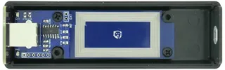
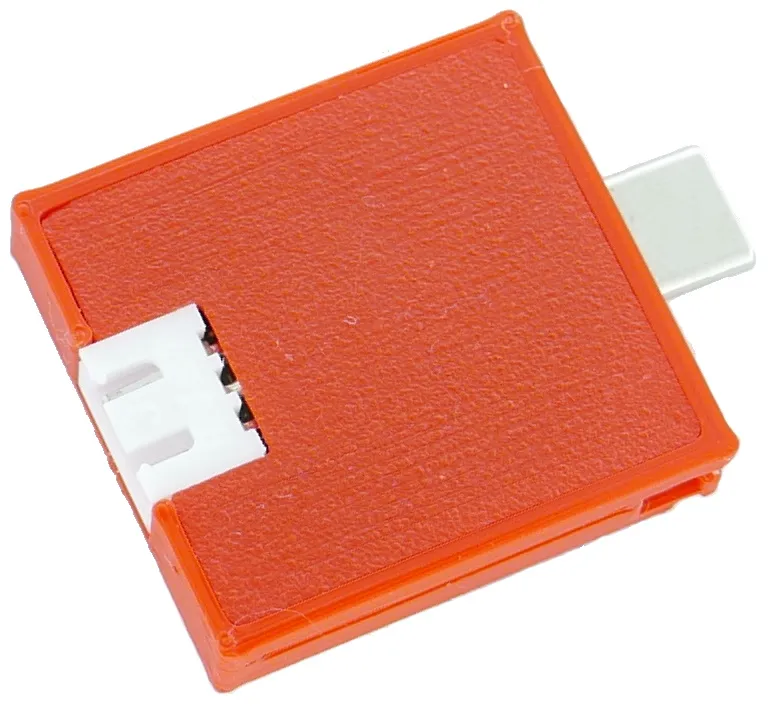
Choosing the enclosure was the easiest part. I saw this project fitting perfectly in Hammond 1593DBK. Its long format gives me enough space for antenna while its shape just calls for a watch to be placed around it. Even better, if I cannot get the original, there is an extremely similar HP-3653-B from Bud Industries.

Mind you, they are not exactly the same. For example, one has screws on the top while other has them on the bottom. Bud has just a smidgen shorter length. Even the shape of the panel is slightly different. So you cannot really just get PCB designed to fit Hammond directly into the other. However, if you are aware of those things, you can abuse tolerances a bit and design both board and panels that fit either case without any noticeable difference.

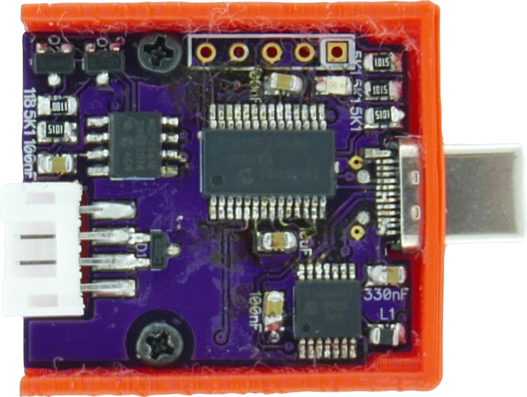
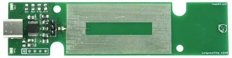
At first I decided to have a 0.8mm PCB so my favorite type-C can be easily soldered. PCBWay generously offered to get them to me for free. While this wasn’t the first time I ordered from them (and yes, I paid for boards more times than I got them free) it was the first time I used them for 0.8mm board.

Illustration

They have a crazy amount of options and I keep changing my mind about how user-friendly this is. For some projects it makes sense to go over many options and fully customize everything but having all options on one page is slightly overwhelming and selecting the “wrong” option can really increase the price. If you don’t catch it immediately, it might be hard to figure out which option changed the price. Fortunately, both 1.6mm and 0.8mm are the same price. While some colors do involve extra cost, there is a fair selection of colors you can get for free. I went with green just because it ships faster.

For this project I didn’t go with any extra options and the only thing I missed was gold plating. While their HASL surface was leveled and I didn’t have any issues soldering 0.65mm SSOP components, the “golden” ENIG finish is nicer. However, $35 price increase for such finish seemed excessive and was not worth it for me.

When it comes to how the finished board looks, a basic green PCB is not a looker. While normal 1.6mm boards are a bit translucent, going to 0.8mm makes it excessively so. I cannot say I’m a fan of how it ended up looking and I would go with any other color (love the blue they have), even if it means a few days more.

Also worth it, is the removal of an internal product number PCBWay places on their boards unless you pay the extra $3. The placement itself was unobtrusive and sensibly done (way better than a few years before) but I am not sure if it was due to the care or pure coincidence. Even so, I think not having that number should be the default (and free).

My board didn’t push any limits (8/8 mils) so I didn’t really expect any issues. And I must say I saw none. The quality was good with traces looking really even. Based on just that I can bet their process is quite better than 6/6 they offered as a default. Either way, hand soldering 0.65mm SSOP was not troublesome at all. Not only traces and their solder masks were perfectly aligned but also surface didn’t have any serious leveling issues. I did notice there were some leveling artefacts (more on those later) but they seemed to be purely visual.

Interestingly, something went wrong with board sizes once I uploaded gerbers and my board suddenly became smaller as the order was placed. Their support did notice the same and we managed to sort it out but it caused a small delay. And yes, it was repeatable as board I ordered some time later (non-sponsored) had the exactly same issue. It might have been that their parser had issues with my DipTrace gerbers but I didn’t notice anything suspicious in them.

In any case, the boards arrived quickly. Some might say too quickly as I was still waiting for my microcontroller of choice - PIC16F1454. And I waited. And waited. Yep, I got hit by a chip shortage. But eventually Microchip came through (yes, I had to order directly from them) and the chips were in my hand.

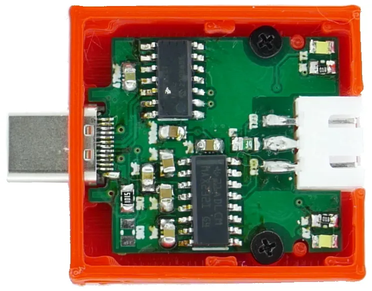
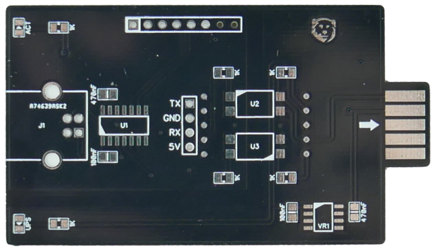
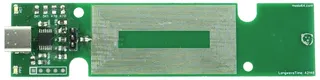
PCB design itself was reasonably simple and only about a fifth of board was used by components. The heart was already mentioned 16F1454 with an USB connector on one side and an antenna output on another. And I simply love this microcontroller.

If you want to make a serial USB device, it’s hard to get it easier than this. The only extra components you need for everything to work are two capacitors; one for general decoupling and one for the built-in USB module regulator. No external crystal, voltage regulator, nor USB pull-ups. That leaves fair 9 pins for general I/O.

Considering I just needed USB communication (D+ and D- pins), PWM module to generate 60 kHz, one output to modulate antenna signal, and another to blink a LED, even this microcontroller was more powerful than needed. However, if I needed some other features (e.g. ADC), its pin-compatible brethren - 16F1455 and 16F1459 - would allow for some growth before going to a completely different device.

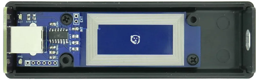
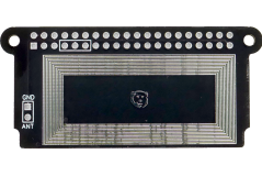
The most notable board feature is, of course, its rectangular PCB antenna. First of all you should understand that realistically you cannot create a good 60 kHz antenna on a PCB. For such a low frequency you need a LOT of wire and this PCB is way too small to fit so many loops. Even if I could fit all these loops, a PCB is not a friendly environment for it. Not only putting wire loops in a close proximity will make an inductor but it will also make a capacitor and a decent resistor.

Even if you cajole inductance and capacitance to get it to resonate at a right frequency, the amount of resistance all those trace loops have would force us to use a proper antenna driving circuit and not just a few resistors you see here. Even with all that, the imperfections in PCB process would make it impossible to retain all parameters from board to board as even the smallest trace change would throw it out of whack. And remember, we’re talking here about impractically big PCB to start with.

However, since I was intending to use this antenna in a close range, a lot of things don’t matter. Having such a huge mismatch actually helps with preventing signal going to far and messing with devices further away. It also doesn’t matter if antenna has solder mask removed or not. For this board I decided to go with solder mask removed but looks are literally the only reason for that decision. At 60 kHz this solder mask simply doesn’t change anything.

Illustration

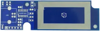
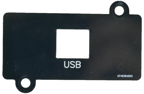
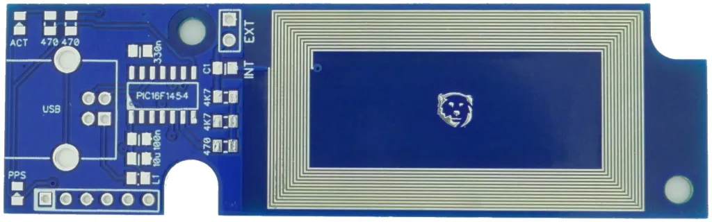
While waiting for components to arrive, I also decided to trim board a bit and make it easier to solder as not everybody likes SSOP and a type-C connector. This variant was a standard 1.6mm, slightly shorter in length, and with some components moved around a bit. And yes, I got it too from PCBWay but I paid for it with my own money . Regardless, the service I experienced was the same (including support for gerber size issue). The only change was a definitely nicer blue color - well worth extra few days of waiting if you ask me.

One extra thing I noticed about the blue board is that antenna looks much nicer and more leveled when compared to the green PCB. While the green board seemed leveled enough, on photos (or if you turn it slightly under the light), antenna has what looks as a “wave” across its surface. The blue board has the antenna surface looking much more leveled and without such artefacts.

I did check boards I previously ordered from PCBWay and I don’t see similar issues. My best guess is that their HASL leveling is not really optimized for 0.8mm boards and when you combine this with a slightly transparent (and thus less forgiving) green board you get visually worse result. Mind you, I only noticed it once I took photos under bright light so it’s really not a big deal.

In any case, with the board ready, it was time to do the firmware…


Please note I have received PCBs for this project for free from PCBWay and they are also the current sponsor of my website. They didn’t request anything specific for me to say and all opinions given here are mine and mine alone.

Longwave Fun (part 1; aka HAT)

This is a part 1 in my WWVB time signal series (part 2).


Illustration

I have been aware of “atomic” clocks and watches for a while now. Those devices rely on WWVB signal (at least in USA) for occasional time synchronization. Between two synchronizations they depend upon a standard quartz crystal to keep time. This allows for decent accuracy almost assuring time is always within a second of precision.

So, this year I decided to jump on that particular band wagon with a Casio Lineage watch. And I was immediately hit by a disappointment. While watch itself was exactly what I wanted, I simply couldn’t get it to receive and decode WWVB signal during the day. Night was slightly better and I could get it synced in the wee hours. And yes, night-time synching is what watch does anyhow and for any normal person that would suffice. But me? I wanted to play with it.

So I went searching for a WWVB transmitter. And it took no time to find Radio time station transmitter by HennerZeller. It worked wonderfully using nothing more than three resistors and a loop of wire. Instead of leaving the perfection alone, I decided to mess a bit with it.

First of all, I decided to put all components of HennerZeller’s design onto a PCB. Already with this change things got even simpler as the only external element was the antenna wire. So I attempted to remove even that using PCB trace. And here comes the first issue - if you want to make a proper antenna for WWVB at 60 kHz, you need quite a long trace. About 1.25 km for the quarter length. A bit too much for a PCB.

However, same principle as in the original design applies. If you’re ok with making a really bad antenna, any loop will do. And bad antenna has unexpected benefit - it will limit range of transmitter. Since we want to keep emissions under 40 μV/m as measured at 300 meters in order to keep FCC happy, having an imperfect antenna is really a good thing. Moreover, since watches were designed to work with weak signal, better antenna might cause issues at close range.

It did take me a few tries to figure out the exact geometry to make it work. I found that 13 loops in rectangular area allows for up to 10-20 cm (4-8 inches) of working distance. If more distance is required, PCB also includes a connector for external antenna. While transmitting longwave is troublesome, one could look into a loop stick or even a spiderweb antenna.

When it comes to PCB, one thing that immediately grabs attention is its wonky shape. Overall dimensions were clear to start with as I wanted to match Raspberry Pi zero footprint. And as long as one makes 65x30 mm rounded rectangle PCB, you have it. Since full size Raspberry Pi can take smaller boards, one would think that there’s no need for messing with it further. Until you try to put it into the official Raspberry Pi case.

Due to how the official Raspberry Pi case connects together, rectangular PCB hits side pillars and prevents it from closing. Further more, there is a camera connector underneath it so notch is needed to allow easy routing. Due to both these issues, the actual PCB got a few curves and a slim down on sides where it would interfere thus giving it the final shape.

The end result is a WWVB transmitter fully compatible with HennerZeller’s design and software fitting nicely into an official Raspberry Pi case.


PS: While this device complies with FCC rules for low power transmitters, that doesn’t make it legal in every other country. Do your research before using it._

PPS: If you’re interested in building your own, you can grab source files from GitHub or purchase kit here.

Overthinking UART Pinout

Quite a few of my boards have a 4-pin UART output. And it’s always the same: [TXD GND RXD VCC]. But this pinout seems strange to quite a few people. I promise, there’s a method to the madness.

First of all, what is the most common UART pinout and why don’t use it? Well, the most common output I’ve seen on other people boards is [VCC RXD TXD GND] and I hate it because it’s really unforgiving if you accidentally plug it the wrong way. When I started playing with electronics, I used to use this pinout and, after frying a couple of boards, I’ve learned to triple-check that I don’t plug it rotated 180°. Even so, it still makes me nervous.

The other common pinout I’ve seen around is [VCC GND RXD TXD] and this one is slightly better as you can safely rotate it 180°. When it comes to common accidents (180° or off-by-one), it’s really hard to fry the board using this one. But this pinout also has its twin brother [VCC GND TXD RXD] thus ensuring you need 1x1 Dupont connector for each wire.

For my “standard” pinout I wanted to be able to easily switch TXD and RXD lines. Since UART really needs only three pins, it was clear that the first three pins had to be [TXD GND RXD]. This way rotating 180° allows you to connect two cables together allowing for point-to-point connection.

In order to provide power, I just added the extra pin for the final [TXD GND RXD VCC] pinout. If you accidently rotate it 180°, nothing happens. If you plug it off-by-one, nothing happens. And, if you don’t need power, you can plug only the first 3 pins and everything still works.

It’s as full-proof as it gets for me.

Calculating Mean for Microchip PIC

Illustration

Averaging ADC readings on microcontroller is often needed but also often quite problematic. The easiest way to do it is remembering the last N values, summing them together and simply dividing by count. Simple, reliable, and uses a BUNCH of memory. If you want to store 50 16-bit values, you will need 100 bytes. When dealing with Microchip PIC, that’s a fortune.

However, if you’re ok with a mean rather with an average, there’s an easier way (and I would argue that mean is a better measure anyways in 90% of cases). You can use Welford’s online algorithm to get mean value using only 3 bytes of static storage and a few bytes more when executing. Of course, use of such algorithm in microcontroller environment will require a bit of a trade off (the least of them is me using average and mean interchangeably further down in post).

For my case, I assumed I need it for unsigned 10-bit ADC values. In the context of Walford algorithm, this means my intermediate values can be up to 15-bits (16-bit signed integer is needed internally) and this leaves 5 bits to use as a fixed decimal point. My case also called just “averaging” a handful of values, so I was ok with a 8-bit counter.

This means my variables are as follows:

uint8_t walfordCount = 0;
int16_t walfordMeanEx = 0;

As compared to the standard Walford’s algorithm, a few things are different. First of all, if we have more than N entries, it will reduce count to half over and over again. This trickery is allowing for “sorta” running average. And yes, you shouldn’t really use Walford’s for running average but it’s close enough. Secondly, when adding the value into the internal variable, we convert it to the signed integer and shift it 5-bits to simulate a decimal point. The only expensive (in CPU terms) operation here is dividing by count as everything else is quite cheap (shift, subtractions, and comparisons).

void walford_add(uint16_t value) {
    walfordCount += 1;
    if (walfordCount > WALFORD_CUTOFF) { walfordCount >>= 1; }
    int16_t delta = (int16_t)(value << FIXED_DECIMAL) - walfordMeanEx;
    walfordMeanEx += delta / walfordCount;
}

To get a value out, we just shift variable 5-bits back to remove the “decimal point”.

uint16_t walford_getMean(void) {
    int16_t value = (walfordMeanEx >> FIXED_DECIMAL);
    return (value > 0) ? (uint16_t)value : 0;
}

And that’s it. It’s a cheap (memory-wise) way to get an average on a 8-bit microcontrollers. As compromises go, I had worse.

In any case, you can download code here.

Why My Serial Port Device Is Detected as a Mouse

When designing electronics, probably the easiest way to make it communicate with a computer is to connect it as a serial port. However, occasionally you might see your device detected as a serial mouse instead of a plain serial port. When this happens the device will obviously not work and you might even see your mouse cursor jump around.

This behavior is an artefact of how Windows detect a serial mouse since that was written way before plug’n’play times. Widnows will first raise DTR and RTS signals and then monitor if there’s an M or B character coming at 1,200 baud. If either character appears, congratulations - your device is now a mouse. And anything it sends will be processed as if it was a mouse action.

There’s a brute force solution of disabling serial mouse in registry and that would honestly be the easiest way around. However, what if you cannot modify the registry? What if you need to make your device work in the face of an unknown machine? Well, there are certain tactics you can employ to either make this behavior unlikely or avoid it altogether.

The simplest solution of not sending M or B will unfortunately not work as easily. Yes, if your device works at the 1,200 baud rate, avoiding those characters will be fine. But if your device works at faster baud rate (and it probably does) the other end receiving at 1,200 will misunderstand its output. Depending when the actual bit sample is taken and what your device is actually sending, you might see an offending character appear either every time or every 10 times. Even worse, the frequency of the issue might change depending on the computer or even the room temperature. So, not really a solution.

The second obvious choice is detecting DTR and RTS combination and pausing whatever output your device gives until that state passes. If you can afford this, it’s a great and surefire way to sort the issue out as DTR and RTS are not baud rate sensitive. The only problem happens when you need those signals for flow control or for something completely custom. Even if you’re not using them they’ll still “cost” you two pins.

The most practical way I found of stopping this issue is by having device not speak until spoken to. If you design your serial protocol so that a device must receive a valid command before it will send any data, it will pass serial mouse detection unharmed. And, if you really need a streaming output (a perfectly valid requirement), just use a command to turn it on. If you can additionally somehow get CRC check into your protocol, the world is your oyster.