Bad things happen when programmer finds a soldering iron

EEPROM Access Routines For PIC18

While I was playing with CAN bus, I needed to write something to EEPROM memory - to keep it safe between reboots. Imagine my surprise when calls to eeprom_read and eeprom_write returned errors:

warning: unsupported: The Read_b_eep routine is no longer supported. Please use the MPLAB X MCC.
warning: unsupported: The Busy_eep routine is no longer supported. Please use the MPLAB X MCC.
warning: unsupported: The Write_b_eep routine is no longer supported. Please use the MPLAB X MCC.

It seems PIC18 series doesn’t support old EEPROM routines that worked on PIC16 but, at the same time, my PIC is old enough not to be properly supported in the suggested MCC. I guess it was time to write PIC18 version of these functions myself.

Reading over documentation for PIC18F25K80, I was pleasantly surprised that EEPROM writing hasn’t really changed. My assembly code I wrote back in PIC16F84 days was quite close to what’s needed these days too. The only significant change was expanding EEADR to allow for more than 256 bytes. Yes, there are some shenanigans with setting EEPGD/CFGS bits but that’s done only once.

My replacement for eeprom_read function was similarly named eeprom18_read and it’s really a drop-in replacement. Not to be the one to dwell in past, I opted to change my ASM code to XC8 flavored C. It’s essentially just setting up EEPROM address, followed by read request, a short pause to get the data, and then reading the data itself.

unsigned char eeprom18_read(unsigned int offset) {
  EECON1bits.EEPGD = 0; // accesses data EEPROM memory
  EECON1bits.CFGS = 0;  // accesses data EEPROM memory

  EEADRH = offset >> 8;
  EEADR = offset;

  EECON1bits.RD = 1; // initiates an EEPROM read
  Nop();             // it can be read after one NOP instruction

  return EEDATA; }

Writing was a bit more involved but not too much so. After setting EEPROM address and data, it was important to allow EEPROM write and disable interrupts as ancient EEPROM unlock sequence (0x55 0xAA) must not be interrupted. After write is initiated, code will wait for it to complete and then restore interrupts. For safety it will also disable further writes to EEPROM until it’s needed again.

void eeprom18_write(unsigned int offset, unsigned char value) {
  EECON1bits.EEPGD = 0;  // accesses data EEPROM memory
  EECON1bits.CFGS = 0;   // accesses data EEPROM memory

  EEADRH = offset >> 8;
  EEADR = offset;

  EEDATA = value;

  unsigned char oldGIE = GIE;  // interrupts be disabled during this code segment
  GIE = 0;

  EECON1bits.WREN = 1;  // allows write cycles

  EECON2 = 0x55;  // write sequence unlock
  EECON2 = 0xAA;  // write sequence unlock

  EECON1bits.WR = 1;     // initiates a data EEPROM erase/write cycle
  while(EECON1bits.WR);  // waits for write cycle to complete

  EECON1bits.WREN = 0;  // disable write
  GIE = oldGIE;         // restore interrupts
}

PCBWay

Illustration

Creating hardware projects usually involves a lot of time spent creating PCB design and then even more deciding which prototype service to use. When PCBWay approached me to consider their service, all I could say is heck yeah. :)

The first thing you’ll experience ordering boards from them is a page full of options. While you can select a few simplified “deals” from main page, they will all bring you to this page for customization. And you can customize a bunch. It’s like a prototype service on steroids.

You can select number of layers (up to 14), material (including flex construction), board thickness (0.4 to 2.4 mm), copper thickness (1 to 4 oz), and surface finish (including hard gold - great for edge connectors). Yes, not all combinations are supported at the same time - for example you cannot have 14-layer aluminum board) - but there is enough choices to make you happy and/or crazy.

You can also select track/spacing (up to 4/4 mil) and hole size specification (0.2 mm) with or without plugged vias (great for BGA work). If you click on special option you can further select castellations, edge plating, impedance control, blind vias, the list goes on and on. If you need it, chances are you can order it. A more “standard” customization of solder mask and silkscreen color almost goes unnoticed.

All these options do come at price. Not only the cost of board can go into hundreds of dollars but it also makes the whole process way more complicated than what you’ll need 99% of time. Clicking on various options can get you so sidelined that you’ll forget about the most basic stuff.

For example, I managed to order all my boards without ENIG finish (immersion gold) just because I somehow missed that option. I would kill for a few simple templates with the most logical options preselected (e.g. ENIG for surface-mount soldering) and with only limited customization allowed (e.g. solder mask and silkscreen color). Yes, there are “specials” available but they still end at the same overly-complicated page.

Upload process is rather pain-less and even supports my favorite RAR format. I used the exactly same files I usually use with OSH Park and PCB:NG service without any issue. Unfortunately, there is no gerber preview here so you might be up for a surprise if something goes wrong.

As one has to define size for board during upload, I intentionally selected a smaller size for one of them. Person doing verification caught it and corrected both board size and the price. This gives me hope that any gerber errors might be caught too but note that such manual review will probably happen a few hours after the upload. This means delay for any issue not easily correctable. I would consider first uploading gerbers to OSH Park and using their awesome preview to perform a sanity check.

Combined with overly extensive customizations, lack of preview makes service much harder for hobbyist (such as myself) to use and I believe even professionals don’t care/need about most of these options on a regular basis. Even when such extensive customization is needed, I doubt one would prefer to go from scratch each and every time.

It takes a few (five in my case) days for boards to get produced but then comes the longest part - shipping. As PCBWay is in China, this means that any cheap shipping will take a while. The cheapest option actually took 2 weeks to arrive, making it slightly slower than US-based competitors. Of course, this assumes you are in States. For international customers timeline might not differ as much. Moreover, there is option for courier shipping but at a significant premium.

Once boards arrived, I found a few things in common to all - most noticeably v-groove routing for external edge. It makes board much cleaner and without any sharp edges to deal with. Boards themselves come either vacuum packed or in a baggie for the small sizes. While vacuum packing might be a bit annoying to open, it does protect the boards quite well in transport.

I immediately hated the addition of order number to the silk screen. While it seems engineer took care to place it underneath big components where it wouldn’t be visible, it’s kinda lottery if you need a really clean look (e.g. customer facing panel). If you note where their number can and cannot go on the silk screen in the comment field, I am reasonably sure they will cautious. However, such instructions are an extra step you need to remember and there is still some risk the number will be written right where you don’t want it.

Testing consisted, as usually, of hand-soldering the boards using Hakko D-888 soldering iron. As I use lead-free solder, the temperature was set to (rather low) 350 °C most of the time. All fine-pitch soldering was done by flooding all pins with solder and then wicking the extra away.

Illustration

First board I got to solder was TmpUsb. It’s a small board with all SMD components and white solder mask did look awesome initially. As I went soldering, I noticed a residue forming whenever I touched the solder mask. Not only this sticky residue was ugly to see but it also stuck to the tip. As this was actually my first board with white solder mask, I am not sure if this is something common for that color or PCBWay uses a formula that’s not particularly heat resistant. In any case, not ideal for soldering iron work.

Second board was for Binarko. Not only this board has a fine-pitch component (0.2 mm TQFP-48) alongside quite a few 0603 passives but it’s intended to be press-fit mounted into the case. The good news is that fit is as close to perfect as it gets. Use of v-groove also means there are no breakout tabs to get rid of resulting in much cleaner look. Since I forgot the HASL coating, getting microcontroller aligned was a bit of challenge. Interestingly, the black solder mask handled high temperature much better than it’s white counterpart making much less mess.

Fine-pitched PIC meant I had to use solder wick a lot and that has shown another issue - it’s really easy to lift a trace. When it happened the first time I played around a bit and noted this seems to be related to the temperature. While I didn’t seem to have issues dragging 300 °C tip, at 350 °C dragging soldering tip was much more destructive.

The final board was of UsbAmps. With 0.25 mm pitch TQFP-44 package, it was a bit easier to solder. It’s green solder mask did its work well and I haven’t noticed any heat-related residue. However, sensitivity of traces to heat/dragging remained.

To conclude: If you are still using lead solder or you do reflow soldering, there are no major downfalls considering this service. While it might not be as cheap as OSH Park or PCB:NG for smaller boards (especially considering shipping is not free), it does get better with larger sizes. If board color or a bit more involved customization is necessary (think filled or buried vias), suddenly this service makes real sense. Yes, you are paying a bit (sometime quite a bit) extra but you do get something not commonly found in prototype market.

Default selection of lead HASL finish and paying extra for lead-free or ENIG is a bit of nuisance for me as I prefer poisoning my self with more fancy stuff but it’s probably not a problem for many considering the love hobbyist market still shows toward the good old 60/40.

There is quite restrictive service offered by OSH Park and PCB:NG where selection of anything other than 2 or 4 layer process is simply not possible but you get your board quickly and at a reasonable price. On the other hand there is almost infinite possibility of customization PCBWay embraces but not without the cost.

Now, only if they would stop adding their numbers to boards…

PS: I was given boards for free by PCBWay. I don’t believe that affected my review, but I believe it’s fair to disclose. :)

[2018-08-16: It seems that PCBWay decided to add extra $3 charge if you use PayPal and you will only see it on the last page. Not nice… :(]

[2019-11-24: At this time PCBWay asks you to pay extra $3 if you want your boards without their custom number. Essentially you are paying for them not to deface your board. Nickel and diming…]

Average Number of Lighted Segments on 7-Segment Display

For a project I am doing with kids we decided to use 3-digit 7-segment display. As we intended to video the project (eventually), it was easy to make decision that we’re gonna drive every digit fully - no multiplexing. Not only that simplifies programming logic but it also makes display rock steady during video - no flickering here.

However, with so many pins to drive, I got a bit scared about maximum power consumption MCU would need to deal with. Assuming we go with 10 mA per LED, what is actually the maximum current we’ll need?

The easy answer is 7x10 = 70 mA per digit, bringing it to 210 mA total. Assuming all digits are fully on (we haven’t used decimal point - otherwise it would be 8) we would indeed need that much current. However, realistically, are we always going to have number 8 on display?

For this purpose, we’ve gone and created a table - how many segments we actually use for each digit:

DigitSegmentsCurrent
0660 mA
1220 mA
2550 mA
3550 mA
4440 mA
5550 mA
6660 mA
7330 mA
8770 mA
9660 mA
Median550 mA

As you can see, the most common result ended up 5 segments being lighted. This tells we actually can usually count on 150 mA of precious current needed.

But wait, since our project will count from 0 to 255, we actually won’t have all our digits on all of the time. We need to calculate how many segments we actually have lighted for numbers that we need. An eternity in Excel later we’ve found that median current needed (assuming random distribution) was 120 mA. Maximum was 180 mA (darn 208!) and minimum was 20 mA.

While 180 mA is not trivial, it is definitely less than 210 mA we originally had to count.

100 MA Is a Myth

A lot of electronics ends up being connected to USB - whether they need computer or not. USB and its 5 V has became an unofficial standard power supply for the world. And thus it makes me crazy when I hear from people that you can only draw 100 mA from USB without going through USB enumeration else something horrible is going to happen. And that is bullshit.

Yes, there is such a thing as USB negotiation where each device can request certain amount of current from its host. Older USB devices could ask for up to 500 mA (in units of 100 mA) while USB 3.0 devices have maximum of 750 mA (in units of 150 mA). If you go higher than that, you get into the category of USB Power Delivery 3.0 and the beauty of multiple voltages we’ll conveniently ignore here, and deal only with 5 V requirements.

A misconception when it comes to USB negotiation is due to ability of USB devices to self-report their maximum usage and likewise the ability of chipset to say no if multiple devices go over some internal limit. Ideally, if you have four USB ports on the same power bus with total of 1 A available and you connect four devices using 300 mA each, three would get positive response and fourth one would get their request denied.

What might not be completely clear from this story is that bus has no means to either measure current or to enforce device’s removal. This whole story depends on the device accurately reporting its (maximum) usage and actually turning itself off if it receives “power denied” response. And yes, this self-reporting works as well as you can imagine it. As there is no way for computer to ensure either accuracy of data or device’s compliance everybody simply ignores it.

Computer manufacturers decided to save some money and not verify device’s consumption. So what if device that reported 300 mA is using 350 mA? Should you disconnect the device just because it uses lousy cable with a big loss? Why would you even care if that is the only device connected? What to do if that device just goes to 500 mA for a fraction of second? What to do with devices reporting nothing (e.g. coffee heaters)? Is nitpicking really worth bad user experience (my damn device is not working!) and is it worth extra cost to implement (and test)?

While there were some attempts at playing “power cops” in the early days; with time all manufacturers decided to over-dimension their power bus to handle more power than specification requires and simply placed cheap poly-fuse on it to shut it down in the case of great overload.

Such friendly behavior has culminated with each port of any laptop made in the last five years being capable of 1 A minimum. And you can test it - just connect data lines (or use UsbAmps’ high-power option) - and you will see you can easily pull 1 A out of something officially specified for half of that. And that is without any power negotiation - courtesy of the USB Battery Charging specification.

This leniency from manufacturers in turn generated a whole category of completely passive devices. Why the heck would USB light have a chip more expensive then all other components together just to let computer know its power usage? That is just wasting money if you can get power out of it whether you inform it or not.

Devices that have to communicate with computer over USB kept their self-reporting habits just because they had to use a bit smarter chips to interface the USB. And all those chips had to have power negotiation built-in to be certified. There was literally no cost in using this feature.

And even then they would fudge the truth. Quite often an external CD drive or hard disk would actually need more than 500 mA to spin up. And there was no possibility in the early days to specify more than 500 mA. So they lied.

Such (lying) behavior was essentially later approved with the USB battery specification that uses not an USB message but voltage levels as a limiting factor. It essentially says that you can pull as much as you want while voltage levels are high enough. Once voltage starts dropping, ease off a bit. This point can happen at 1 A, or 1.5 A, or 2 A - it all depends on power source/computer you are using.

Device manufacturers have become quite verse too. Since USB battery charging specification was done is hardware friendly manner, there was no extra cost to bear. Only task was to determine if computer supports the, then new, specification. If yes, pull current until voltage start dropping. If not, limit yourself to 500 mA. How do they recognize it? You’ve guessed it - by shorting the data lines.

Due to the powers of backward compatibility you can pull essentially as much current as you want from your PC. Yes, you are still limited by fuse (quite commonly 2 A or more per port pair), you still have thin USB cables and their voltage drop (with accompanying losses) to deal with, and yes devices - especially phones - will still self-limit to avoid tripping aforementioned fuse. But otherwise it is a wild west.

Unless you are making device that has to be certified, stop worrying about the power negotiation. If your device already has an USB transceiver onboard and you need to program it anyhow, go for the standard and configure current you need. But if you don’t have such chip or programming is just too much of a hassle, simply ignore it and world is not going to self-destruct. I promise.

RetroHat

Illustration

Raspberry Pi is often used for retro-arcade machines. It really fits well there: low power usage, reasonable emulation software support (it is based on Linux after all), more then capable processor, and really cheap price ($35). It is hard to beat this.

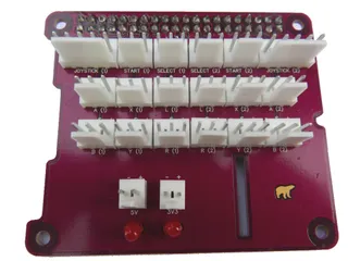
What surprised me is that I couldn’t find proper Raspberry Pi HAT that could be used to treat buttons as a keyboard. Yes, there are guides how to setup buttons, but they don’t do auto-detection and require a bit too much setup for my taste.

There are also USB devices to which you can connect buttons but I find them a bit annoying to deal with in physical sense. While they do offer huge amounts of buttons, them sticking out of Raspberry’s side is always ugly to see.

What I wanted to build was maximum amount of buttons I can get away with using only natural HAT connections and without the need for any driver not available out-of-box. Of course, it should be a proper HAT with EEPROM, auto-configuring everything needed as soon as machine is booted.

First of all, with number of available pins on HAT connector it became clear there is a hard maximum at 24 buttons. Assuming 2 players, that comes to a joystick and 8 buttons (A, B, X, Y, L, R, Start, and Select) per player.

As HAT gives you quite respectable surface to work with, connectors for these buttons could also include a LED support at the cost of few resistors. Moreover, a discrete (fused) connector for both 5 V and 3.3 V rail was added. While neither is intended for heavy use, it comes in handy for powering various extra components in your retro-cabinet.

For keyboard emulation, this HAT uses a built-in support for GPIO keys. As long as you connect momentary button between GND (-) and pull-up input (S) it will detect each press as the transition from high to low and simulate the appropriate button. Default keyboard configuration is selected in such manner that player 1 configuration matches default RetroPie settings while all keys for player 2 are assigned numbers 0 to 9.

Of course, you can configure all this just by modifying retrohat.dts, a file whose creation took probably more time than board design, soldering, and everything else. But it was worth it to get auto-configuration running once EEPROM is programmed. To get more information on how to program the auto-configuration EEPROM, you can either go over read-me file or check how I did it for Cananka.

In any case, check project’s page for a short description and to find link to source files so you can build your own.

OshPark Vs PCB:NG

For feeding my electronics addition I mostly use OshPark. They have quick turnaround, excellent user service, and price is quite acceptable.

However, they are not the only game in town. Probably the best alternative if you are willing to wait a bit is unsurprisingly in China. Yes, I am speaking about Seeed Studio’s Fusion PCB. It is not exactly comparable to OshPark but it is close enough for many purposes. And it is excellent choice if you need different PCB colors - something OshPark doesn’t offer.

But times are changing and there is a new challenger on US soil - PCB:NG. They are PCB assembly house - something that is a bit too pricey in low quantities and something I personally never needed. But they do offer a possibility to order only PCBs.

PCB specifications are quite high-end: ENIG finish (I love this), 4/4 mil traces (vs 6/6 for OshPark), 8 mil vias (vs 13 mil), and they generally support cutouts and slots (although no promises here). As I generally don’t go lower than 8/8, I find them working equally well for my use case.

Price is $6 per inch for 6 boards, compared to $5 per inch for 3 boards OshPark offers - quite similar if you only need a few but PCB:NG wins at higher quantities.

Order process is simple enough and I had no issues with DipTrace 3.0 produced gerbers - something that might fail occasionally with OshPark (e.g. my PCB bear). I would say parser is definitely more forgiving with PCB:NG. I kept all file names setup as for OshPark and there were no issues. Your mileage might vary but I don’t expect anything unsurmountable as you can correct auto-detection yourself. And no, neither PCB:NG nor OshPark support RAR.

First thing you’ll notice when you get a board is attention to packing. There is a nice layering of red paper between each board and there is virtually no chance of them scraping one another. While I am not sure that matters as I never had any issues with loose boards arriving from OshPark, this does look a bit nicer.

What you will see after unpacking is a dark red colored board. I have ordered two within a few weeks and shade is a bit different. It is similar experience to year’s back when OshPark was testing other factories - I am sure shade will become constant very soon if it is not already. Just be mindful if you need exactly the same shade to order all boards at the same time.

All boards come fully broken out - unlike with OshPark where you can still see breakout tab pieces. Tabs themselves seem nicely defined and PCB:NG puts less of them than OshPark. Generally I have less work filing the rough edges then with OshPark. Somebody less nitpicky would be able to use them without filing altogether.

Silkscreen is not bad but white on red makes it less visible than white on dark purple OshPark uses. If you need good silkscreen visibility (e.g. user visible panels) you should probably go with OshPark.

I am not sure whether it was a fluke or standard practice but PCB:NG placed their custom markings on my silkscreen. This is something done by Seeed Studio and most low-cost services as it makes their process a bit easier. OshPark doesn’t do it and I was surprised when I saw PCB:NG doing it. However, on my second board I had no custom markings so they seem to have abandoned this vandalism.

When it comes to copper quality I can really say nothing bad about either PCB:NG or OshPark. Both have nice ENIG finish, neither had issue with traces or solder masks, both can handle hand lead-free soldering without much trouble. If there wasn’t a color difference, I wouldn’t be able to tell them apart.

For me it comes to two things. If board is meant for user visible panel (e.g. end panel for plastic enclosures) I find purple, almost black, OshPark gives fantastic look to a final device.

Where PCB:NG wins is price. As soon as you go over 3 boards OshPark offers, you are better off using PCB:NG. And, if you want some assembly, there is no content at all. PCB:NG is the one that offers low volume assembly.

As I usually do extremely low volume orders (often making just one or two devices) I will probably stick with OshPark. There is something to be said about familiarity. However, PCB:NG is a high-quality contender and worth trying out (remember 4/4 mil traces) - even at a fraction higher cost for a small volume.

Cananka, the Raspberry Pi HAT: Problems

Illustration

[This the last post in the series.]

Mistakes? I’ve made a few…

The very first one was noticed after I’ve already sent order to OSH Park. For back-powering isolation where 2 A are needed, I used the same footprint as for 100 mA DC-to-DC voltage regulator. There is no chance of getting a part that would support 2 A in such a small package. I’ve replaced it with properly sized 1x1" isolated voltage regulator and contacted OSH Park support. As my original order was not sent to fabrication facility yet, I got it swapped with a new design without any additional cost. OSH Park support rocks!

While waiting for a board, I continued going over the design and thus I’ve noticed I’ve forgotten to pull-up the reset line. Uncaught it would cause chip not to function so respin was definitely needed. Additionally I’ve changed layout of board a a bit alongside making a slightly bigger cuts to allow for official case to carry the board. I find it amusing that HATs made in accordance with official specification don’t fit the official case. :)

What I didn’t catch was that my new DC-to-DC brick needs a bit bigger holes. It was possible to get DC-to-DC converter in the board but with a lot of elbow grease. Definitely not what you would want. I also didn’t notice I had damn pinout backward on one side of the chip. And guess what, since I’ve already sent for revision B to be manufactured, I couldn’t change it before revision C.

I did try to mod-wire the revision A of the board but important traces to cut were under the DC-to-DC brick itself so there was no approaching them - not with tight drill holes I had. Fortunately I was able to jump the missing reset line and thus have a proof of concept all is working well.

Revision B arrived when I was already preparing for next revision due to already mentioned faults and thus I have just populated the “cheap” part of the board. It made no sense to mount $25 DC-to-DC voltage regulator if I know it is not going to work. Revision C did have few other changes to silk-screen and other minor changes. Most notable change, outside of DC-to-DC pinout correction, was changing EEPROM to be write protected when WP jumper was soldered over.

Original suggested EEPROM circuit makes write-protection to be default. This means you need to connect the jumper to write chip and then desolder it later to make it read-only. I find it much easier on me if all chips start with being writable and then you make solder bridge to make them read-only. Additionally, as chip has internal pull-up, this means you save a resistor. :)

As revision C came, all seemed great until I tried power-back circuit - it didn’t work. Short troubleshooting later I’ve noticed my reading of remote on/off functionality was lacking a bit and thus I was missing connection of that pin to ground. With that single change power-back started working perfectly. Of course that meant revision D had to be made.

D? No issues what-so-ever. :)

Cananka, the Raspberry Pi HAT: EEPROM

[This post is part six in the series.]

What makes HAT a HAT is its EEPROM. While official instructions are lacking in details there are some forum posts and tutorials dealing with that issue.

In order to follow steps later in this post, we first have to install some packages:

sudo apt-get install git i2c-tools

For HAT EEPROM access we have to tell system to allow use of, usually inaccessible, I2C bus 0:

sudo bash -c 'echo "dtparam=i2c_vc=on" >> /boot/config.txt'
sudo reboot

Easiest way to see if we have set it up correctly is to probe I2C bus 0 for EEPROM at address 0x50 and see what we have there. We are searching device with ID of 0x50:

i2cdetect 0
i2cdump 0 0x50

To manipulate it any further we need to install EEPROM utilities from the Rasbperry repository:

git clone https://github.com/raspberrypi/hats.git
cd hats/eepromutils/
make clean
make

Before anything else is done, it is a good idea to clean out EEPROM:

dd if=/dev/zero ibs=1k count=4 of=blank.eep
sudo ./eepflash.sh -w -f=blank.eep -t=24c32

Now we are finally ready to actually create .eep file from our text config and upload it to EEPROM:

./eepmake eeprom_settings.txt hat.eep
sudo ./eepflash.sh -w -f=hat.eep -t=24c32
sudo reboot

If everything is ok, you should have directory /proc/device-tree/hat with product, vendor, and other files:

more /proc/device-tree/hat/product

But this is not where we want to stop - we want also device tree so that our CAN bus can get some auto-configuration magic. And frankly that whole concept is such a mess that creating it from scratch takes unholy amount of time. However, since CAN over SPI is one of the already existing overlays, we don’t have to do anything other than include it and flash our EEPROM again:

./eepmake eeprom_settings.txt hat.eep /boot/overlays/mcp2515-can0.dtbo
sudo ./eepflash.sh -w -f=blank.eep -t=24c32
sudo ./eepflash.sh -w -f=hat.eep -t=24c32
sudo reboot

Even if our CAN bus implementation didn’t match existing overlay completely (e.g. using different frequency), we could still use it as a template for our modifications. We would first dump it:

dtc -I dtb -O dts /boot/overlays/mcp2515-can0.dtbo > hat.dts

Once we have it in (semi) human readable format, we can change what is needed (e.g. clock-frequency) and then use the same flash procedure as before:

./eepmake eeprom_settings.txt hat.eep hat.dts
sudo ./eepflash.sh -w -f=blank.eep -t=24c32
sudo ./eepflash.sh -w -f=hat.eep -t=24c32
sudo reboot

Now you can remove all modifications done to /boot/config.txt and our interface will still appear:

ip -d link show can0
 3: can0: <NOARP,UP,LOWER_UP,ECHO> mtu 16 qdisc pfifo_fast state UNKNOWN mode DEFAULT group default qlen 10
     link/can  promiscuity 0
 ...

With that, we have Cananka project completed and the only post remaining is to reminiscence over development problems.

Cananka, the Raspberry Pi HAT: Software

[This post is part five in the series.]

One of the requirements I’ve stated was that we should use as much of Linux driver defaults as possible. In this step we should reap benefits of that as all needed to enable CAN should be:

sudo bash -c 'echo "dtoverlay=mcp2515-can0,oscillator=16000000,spimaxfrequency=10000000,interrupt=25" >> /boot/config.txt'
sudo reboot

After reboot, we should see device loaded:

ip -d link show can0
 3: can0: <NOARP,ECHO> mtu 16 qdisc noop state DOWN mode DEFAULT group default qlen 10
     link/can  promiscuity 0
     can state STOPPED restart-ms 0
           mcp251x: tseg1 3..16 tseg2 2..8 sjw 1..4 brp 1..64 brp-inc 1
           clock 8000000

When I was setting this for the first time I was brought on a wild goose chase as nothing really worked. No matter what I did, can0 device would not appear (Cannot find device "can0"). It took me a while to notice something is off:

dmesg | egrep "spi|can"
 spi_bcm2835: disagrees about version of symbol module_layout

As this Raspberry was used for other projects and I’ve updated it multiple times it seems at one point something went wrong with drivers. A fresh reinstall of Raspbian sorted that out.

More careful among you will notice that CAN interface is actually down upon boot. This is easy to correct and the only piece of data we need is the bus speed (this example will use 125 kHz):

sudo ip link set can0 up type can bitrate 125000

ip -d link show can0
 3: can0: <NOARP,UP,LOWER_UP,ECHO> mtu 16 qdisc pfifo_fast state UNKNOWN mode DEFAULT group default qlen 10
     link/can  promiscuity 0
     can state ACTIVE restart-ms 0
           bitrate 125000 sample-point 0.875
           tq 500 prop-seg 6 phase-seg1 7 phase-seg2 2 sjw 1
           mcp251x: tseg1 3..16 tseg2 2..8 sjw 1..4 brp 1..64 brp-inc 1
           clock 8000000

Unfortunately this doesn’t survive the reboot. To make it stick just execute:

sudo bash -c 'echo >> /etc/network/interfaces'
sudo bash -c 'echo "auto can0" >> /etc/network/interfaces'
sudo bash -c 'echo "iface can0 inet manual" >> /etc/network/interfaces'
sudo bash -c 'echo "    pre-up ip link set \$IFACE type can bitrate 125000" >> /etc/network/interfaces'
sudo bash -c 'echo "    up /sbin/ifconfig \$IFACE up" >> /etc/network/interfaces'
sudo bash -c 'echo "    down /sbin/ifconfig \$IFACE down" >> /etc/network/interfaces'

For testing install can-utils:

sudo apt-get install can-utils

With them you can use cansend and candump, e.g.:

cansend can0 02A#FEED
candump can0

At this moment we have are HAT working. However, without EEPROM, we cannot really call it a HAT. So, guess what’s next

Cananka, the Raspberry Pi HAT: Layout

Illustration

[This post is part four in the series.]

The most difficult part of board setup is done for us - we have both dimensions and we’ve decided on components. Even better we don’t need to think about board much as our HAT specification has it all sorted out. Or does it?

If you make board based on HAT specification you won’t be able to fit official case around it. We need additional cutouts if we want it to fit - bigger on the left side and just a small one on the right. As board is not really crowded, it was easy to carve out the additional space. However, it might not be as easy for more dense layouts.

Illustration

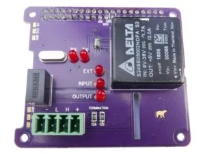
Top side is dominated by our DC-to-DC converter and nice 3.81 mm 4-pin CAN bus connector. Additionally there are through-hole LEDs so we can see activity and a through-hole oscillator purely because I hate SMD ones. To help with troubleshooting a few pads without solder mask are along the edge.

The whole board is essentially split into two parts. On top we can find components that can safely connect to Raspberry Pi. Most notable being MCP2515 CAN bus controller and 24C32 EEPROM needed for HAT compatibility.

Between CAN bus connector and controller we have isolation border crossed only by isolated DC-to-DC converters and ISO1050 CAN bus transceiver. Two millimeter spacing between these two universes should provide adequate protection.

It is a pretty straightforward layout mostly driven by the need to have isolation border and the size of the components.

Now, let’s get the board working.